
I plan to talk about how to make good use of SSDs from the perspective of a storage system architect. The term ‘storage system’ in this article refers to a fully flashed array or fully flashed distributed block.

When I was doing zStorage before, I encountered a problem: the performance testing time was too long, and the amount of data written to the SSD increased, resulting in a decrease in write performance. At that time, I guessed that the SSD backend had started GC (garbage collection), which led to a decrease in write performance. Without evidence, it can only be a guess. Since last year, I have spent a lot of time learning SSD, and now I can confidently say that it is the backend GC of SSD that affects write performance.
This article does not intend to provide a detailed explanation of “why SSDs need to do GC” or “how SSDs can do GC”. There is a lot of content available online, and readers who are not familiar with it can search for it on Baidu or Deepseek and recommend Deepseek. This article focuses on SSD features that I was not familiar with before but have an impact on storage systems.
The write to read performance of SSDs is poor, and random writes are much worse than sequential writes. Now using PCIe Gen5 x4 NVMe SSD, the host interface bandwidth can reach 15.7GB/s, and sequential read can reach 14.5GB/s, but some command overhead needs to be removed. Please refer to the table below for details:
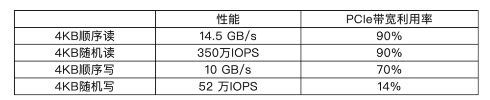
As shown in the table above, the bandwidth utilization of 4KB randomly written PCIe can only reach 15%. Obviously, PCIe interface is not a bottleneck, so where is the bottleneck?
In fact, the bottleneck of SSD’s write performance lies in NAND Flash. The most commonly used TLC Nand Flash in enterprise SSDs now generally requires writing 3 pages of the same WL at once. If each page is 8KB, then 3 pages are 24KB. Writing these 3 8KB pages takes about 700us. That is to say, the write performance of a Flash chip can only reach 24KB/700us=35MB/s. To achieve 10GB/s performance, an SSD needs to be configured with about 300 Nand Flash chips. Looking at SSD photos online, it seems that there aren’t as many Flash chips?
In fact, a single Flash chip usually encapsulates many independent dies (cut silicon wafers) inside, and each die has multiple planes inside, which can execute write commands together. That is to say, it’s not actually 300 chips, but 300 plans. Based on a capacity of 1Tb per die, a 15.36TB SSD requires approximately 140 dies to be configured, with 2 planes in each die. The sequential write performance is approximately 10GB/s. Why is the reading performance so high? Because reading a Flash page only requires 40us. So why is the random write performance (bandwidth utilization of 14%) so much lower than the sequential write performance (70%)?
The main reason for low random write performance is the high write amplification (WAF) caused by GC. If it is written in sequence, then the data on Nand Flash is also overwritten in sequence. All Flash data in a GC recycling unit is overwritten together. Although there is still a GC process, all pages in a GC recycling unit are overwritten, and there are no valid data pages left, so there is no need to copy the data. Therefore, there is no write amplification (WAF=nand_ write. bytes/host_ write. bytes=1.0). If it is a 4KB random write, there are still many valid data pages inside a GC recycling unit that need to be copied to a new location in Nand Flash before the GC recycling unit can be deleted. This copying process will introduce write amplification. If using Fio for 4kb random write testing, some models of SSDs can achieve write amplification (WAF) of 4.5 or even 5.0 under extreme conditions, which means that 5TB of data is written into the NAND flash, only 1TB is written by the host to the SSD disk, and the additional 4TB of data written is generated by the GC replication process.
For example, if the SSD sequential write performance in the table above is 10GB/s and the 4KB random write performance is 520000 IOPS, then the write amplification of this model of SSD under the 4KB random write limit is WAF=10 * 1E9/(52 * 1E4 * 4096)=4.7. The write amplification caused by GC not only results in low random write performance, but also affects the lifespan of SSDs. The main factor causing wear and tear on Nand Flash chips is the number of erase and write cycles, which refers to the amount of data written to Nand Flash.
Is there a way to reduce write amplification in the storage system? One easy way to think of is to change all random writes to SSDs to sequential writes. My opinion on this idea is that there is no need to do so in order to reduce SSD write amplification. If your system is originally designed for append only, then SSD naturally requires sequential writing, such as RocksDB or ZFS, which do not require any special design for append only systems. If the storage system is designed with Update In place, changing to append write can indeed reduce the write amplification inside the SSD, but it cannot reduce the end-to-end write amplification of the entire system, that is, the amount of data written to Nand Flash does not decrease. Because adding writes to SSDs requires adding a GC process to the storage system, which means moving write amplification from within the SSD to the storage system software. From a higher-level application perspective, overall write amplification has not decreased.
The above approach also has another benefit, which is that the storage system can decide when to start the GC process. If you know when the business pressure is low, start the GC process when the business pressure is low, which can minimize the negative impact of GC on performance. The internal GC process of SSD tends to start as late as possible, because starting the GC process later will result in more data pages being overwritten, which will reduce the number of valid pages that need to be copied and write amplification. In my opinion, this benefit is not significant enough and it is not worth changing the storage system to append write for this.
Another issue to note is that if you decide to switch to append write mode, you must do it thoroughly, and the length of the append write data block should be as large as possible.
Generally speaking, enterprise SSDs now perform RAID between Flash chips internally, so that in the event of an error that LDPC cannot correct (such as die failure), data can be recovered through RAID. The GC recycling unit for enterprise SSDs is a Super Block, which forms a RAID group. All corresponding blocks on each die together form a Super Block. One block in this Super Block is used to store parity, while the other blocks are used to store user data. A Super Block will be reclaimed and erased by the GC process as a whole. RAID results in a relatively large size of GC recycling units, for example, the block size of a physical Flash chip is 64MB. If there are 300 blocks in a Super Block that make up a RAID, the size of the Super Block is 64MB * 300=19 GB. If the storage system is changed to append write and uses an 8MB recycling unit for GC, for an SSD with a 19GB GC recycling unit, the upper layer storage system still writes randomly, not sequentially. When doing GC on SSDs, there will be many 8MB holes and 8MB of valid data in a 19GB recycling unit. The GC of SSD still needs to perform data replication, which cannot reduce SSD write amplification.
In addition to sequential writing, TRIM can also significantly reduce WAF. When GC selects a Super Block for recycling, if many data pages in this Super Block are actually invalid but have not been overwritten by new data or deleted by the TRIM command, then the GC process must copy it as valid data pages. If the TRIM command marks this page as invalid, the GC process does not need to copy it and reduces write amplification. The mount command of the ext4 file system in Linux has a parameter – o eject. Adding this parameter during mount will issue a TRIM command to the SSD.
In addition to sequential writing and TRIM, increasing the over provisioning page can reduce WAF. Because the OP space is larger, the GC process can start later, and the SSD can handle more write and TRIM commands first. As a result, there are fewer valid pages in the super blocks selected for recycling by the GC, fewer pages need to be copied, and the WAF will be smaller.
Another method to reduce write amplification is FDP. The storage system first predicts which data has a short lifespan and which data has a long lifespan, and then uses FDP to inform the SSD of the predicted data lifespan. When SSD writes data, it puts data with the same lifespan into a Super Block. This way, when a Super Block is selected for recycling, there are very few valid data pages that need to be copied inside, and the WAF will be relatively small.
Many enterprise SSDs have an FTL granularity of 4KB, meaning that one FTL entry points to a 4KB Nand Flash physical address. If there are many write requests smaller than 4KB in the write operations issued by the storage system, such as 512bytes, then the SSD needs to first read out 4KB of data, modify 512B, and then write back 4KB. This will also affect performance and cause another type of write amplification. But if it is a continuous write of 512B, such as writing WAL logs, this does not affect. Because there is a backup capacitor inside the enterprise SSD, the 512B data written by the host to the SSD will be temporarily stored in memory, and after filling 4KB, Flash will be written. That is to say, the storage system should try to avoid random writes of less than 4KB. In addition, some ultra large capacity (30TB, 60TB,…) QLC SSDs on the market now have an FTL granularity that is not 4KB, but may be 16KB or larger. It is important to avoid random writes of less than 16KB for them.
Some storage systems will immediately read out and perform a check after data is written to the SSD to ensure that the data is written correctly. For SSDs, this approach is not good. Because if the data just written by Nand Flash is immediately read out, Nand will be in an unstable state and the bit error rate will be relatively high, which may affect performance and also cause misoperation of the SSD’s internal read voltage adjustment algorithm. The storage system should try to avoid reading data immediately after writing it.
Does SSD generate bad lanes? Yes, but the reason why SSDs generate bad lanes is different from HDD. The bit error rate of current TLC/QLC Nand Flash media is very high, some can even reach 10E-4, which means that when a 4KB data page is written into Nand Flash and read out, there are almost always a few bits that are incorrect. These errors are recovered using LDPC and RAID algorithms, but SSDs cannot guarantee that data will always be recovered. In the event of an unrecoverable situation, the data at this LBA address can only be marked as a bad lane. Unlike the bad lane in HDD, rewriting the LBA address of this bad lane restores its state and it is no longer a bad lane.
When I was working on zStorage, I was once troubled by a question: if I encountered bad lanes while reading an SSD, does it mean that there are still many bad lanes in this SSD? Do you need to perform a full disk scan on this SSD? Do you need to remove this SSD from the system? In fact, the NVMe standard provides a command LBA status, which can return all bad lanes of this SSD to the host. The host only needs to recover and rewrite the bad lane data, without the need for a full disk scan of the entire SSD. Because full disk scanning is quite time-consuming and affects performance. SSDs also perform internal task scanning in the background during startup and mark unrecoverable data blocks. Of course, it is necessary for the storage system to perform a full disk scan every once in a while, as it is the most reliable. If the LBA status command is fully utilized, the time interval for this full disk scan can be longer.
Another point is that the working temperature has a significant impact on SSDs. As the temperature rises, the error rate of Nand Flash will increase, which will affect the performance of SSDs as it takes more time to recover data. In addition, the working temperature also has a negative impact on the lifespan of SSDs, as high temperatures accelerate the aging of the tunneling oxide layer in Flash Cells.


暂无评论内容